 
| Subject: | |
| From: | |
| Reply To: | |
| Date: | Fri, 7 Dec 2012 03:02:38 +0000 |
| Content-Type: | multipart/related |
| Parts/Attachments: |
|
|
Hi All,
大家好!近日實驗室在進行失效分析過程中遇到以下案例,請教發生的原因為何,該如何進行改進?
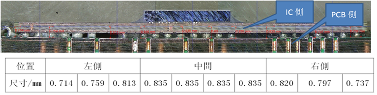
1. 不良現象描述:PCB在Reflow過程中,或維修更換IC芯片時出現PCB下陷,如下為切片分析數據:
[cid:[log in to unmask]]
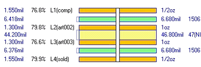
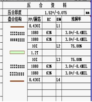
2. 目前該產品有兩款PCB在使用,其中一款未發生類似狀況,一款有發生,所以對其疊構進行分析差異如下:
叠构
問題板 单位 MIL
正常板 单位 MIL
差异
Layer 1铜
0.7
0.602
Layer 1 铜厚不同
PP
6.68
6
問題板1506 pp 1张,含胶量48%;
正常板1080 PP 2张,含胶量63%;
Layer 2铜
1.4
1.4
/
PP
46.8
47.24
基板PP厚度不同;但是TG均≧135℃
Layer 3铜
1.4
1.4
/
PP
6.68
6
問題板1506 pp 1张,含胶量48%;
正常板1080 PP 2张,含胶量63%;
Layer 4铜
0.7
0.602
/
[cid:[log in to unmask]]
[cid:[log in to unmask]]
BR,
Michael
______________________________________________________________________
This email has been scanned by the Symantec Email Security.cloud service.
For more information please contact helpdesk at x2960 or [log in to unmask]
______________________________________________________________________
|
|
|


